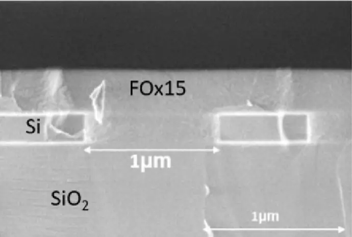
Multilayer photonic platforms require flat, high-quality intermediate cladding layers. We developed a bilayer hydrogen silsesquioxane (HSQ) contact-planarization process that works for silicon etch depths of 220 nm and 300 nm, trench widths from 75 nm to 1 µm and spacings from 50 nm to 3 µm, with residual thickness variations down to about 1 nm. Interlayer transitions between silicon and silicon nitride waveguides show losses as low as 0.3 dB per interface.
Read the paper: Micro and Nano Engineering 32, 100379 (2026), doi: 10.1016/j.mne.2026.100379