
There is an ubiquitous problem that everyone designing, testing, and using integrated photonic devices has to face: how to efficiently get the light in and out of the chip. Exploiting machine learning, we design a solution based on a micron-scale antenna featuring high efficiency and ultra-wide bandwidth.
The difficulties in interfacing a photonic integrated circuit with the outside world come mostly from integration biggest advantage: small dimensions. The sizes of a silicon photonic waveguide are in the order of few hundreds nanometers. As a comparison, optical fibers have a core which is eight to twenty times larger. Light needs to be literally “squeezed” from the fiber into a tiny integrated waveguide. Here we achieve this goal using as antenna a surface grating coupler of only 3.6 microns.
In silicon photonics, grating couplers are devices realized by arranging silicon structures in a periodic (or semi-periodic) way. They allow to diffract light propagating in a waveguide out of the chip. Our grating design has only five periods and exploits as fundamental cell a silicon pillar followed by an L-shaped structure. This particular design is known for its high performances and here provides an upward diffraction efficiency of 92% which translates in a coupling efficiency of 81% (-0.9 dB) for fibers with a mode field diameter of 3.2 microns.
The most interesting thing is that light is diffracted perpendicularly out of the chip plane. This condition is highly desirable because it makes systems assembly much easier but it is very hard to obtain with a grating coupler. The reason is that when light is diffracted perpendicularly, a large part is actually reflected backward in the waveguide due to second order Bragg diffraction. In this case this is avoided by carefully designing the grating structure and the antenna shows a reflection consistently lower than -20 dB over a 200-nm wavelength range between 1450 nm and 1650 nm.
Last but not least, the very small dimensions of the antenna not only allow to design dense and highly integrated circuits but also ensure a huge operational bandwidth. The antenna has a 1-dB bandwidth of almost 20 THz (158 nm). The coupling efficiency only varies by 0.06 dB across the optical communication C band (from 1530 nm to 1565 nm) and 1.3 dB across the S, C, and L bands (from 1460 nm to 1625 nm).
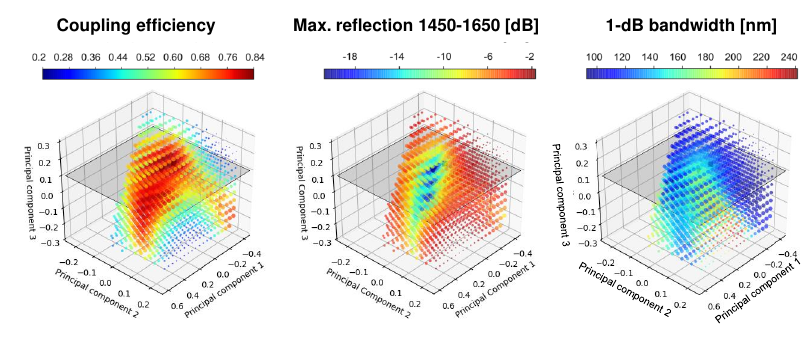
This record-high performances are obtained exploiting machine learning for the antenna design. The approach is based on local optimization, adjoint simulations, and principal component analysis. As a result, the design space is rapidly and exhaustively mapped by parameter sweeps computing not only the coupling efficiency but also any other required performance, allowing a comprehensive analysis of the device behavior. The figure above shows an example of the maps generated during the design. The interplay between efficiency, reflection, and bandwidth can be clearly analyzed.
The result of the design is a micron-scale antenna with extremely high performances which make it ideal for applications requiring dense arrays of both fiber and free-space coupling interfaces.
All the details can be found in the invited paper published by Journal of Selected Topic on Quantum Electronics:
D. Melati et al., “Design of Compact and Efficient Silicon Photonic Micro Antennas with Perfectly Vertical Emission,” IEEE J. Select. Topics Quantum Electron., pp. 1–1, 2020, doi: 10.1109/JSTQE.2020.3013532
A pre-print version on the paper is available on arXiv: arxiv.org/abs/2008.02552