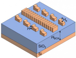
Metamaterials are artificial media realized by arranging building blocks at distances smaller than the wavelength. By properly designing these unitary “atoms” it is possible to engineer the macroscopic behavior of the metamaterials and extend the range of material properties compared to those available in nature. New photonic device concepts have been demonstrated exploiting metallic, hybrid metallic–dielectric, or all-dielectric nanostructures in the form of metasurfaces or bulk metamaterials. Despite their vast potentialities, design of metamaterials can quickly become intractable for the large number of involved parameters, especially if free-form atom shapes or non-periodic arrangements are used. Inverse design and machine learning techniques offer particularly well-suited tools to address this problem. With this approach, we combine new degrees of freedom in controlling material properties offered by metamaterials with silicon-based integrated photonic components and on-chip architectures to demonstrate devices with superior characteristics, e.g., ultra-wide bandwidth, low reflections, large feature sizes, and complex spectral behaviors.
[1]L. Puts, X. Leijtens, P. Cheben, J. Schmid, S. Reniers, and D. Melati, ‘Anti-reflection subwavelength gratings for InP-based waveguide facets’, Opt. Lett., OL, vol. 46, no. 15, pp. 3701–3704, Aug. 2021, doi: 10.1364/OL.431353.