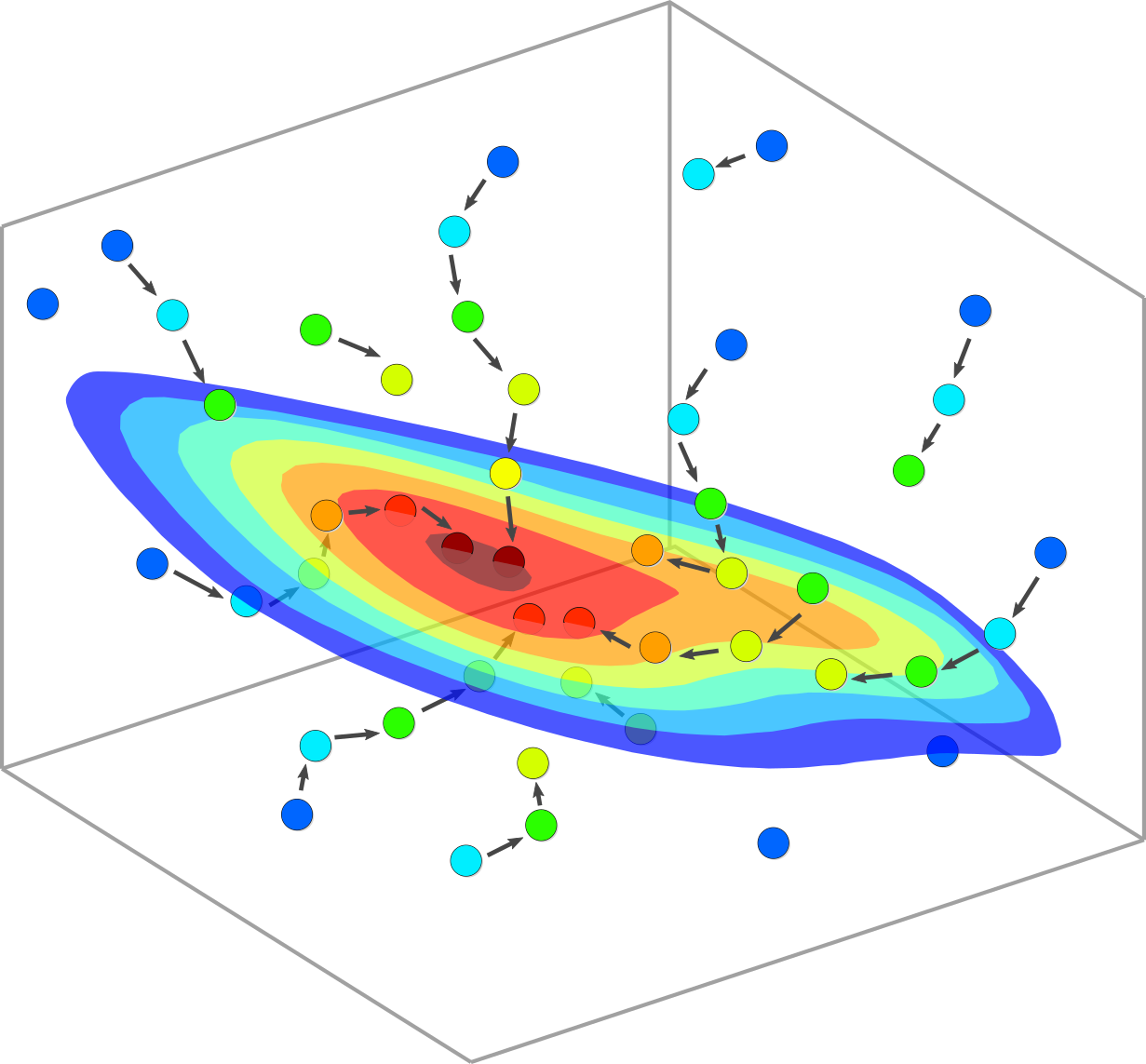
The consolidation of photonic integration technologies is boosting the on-chip integration of advanced devices and the implementation of many functionalities in complex photonic circuits. Despite nanophotonics broadens in complexity and application range, photonic design has largely remained a time consuming process that relies mostly on theoretical knowledge and physical intuition of the designer. This approach is constrained in scope by computational resources and limited to structures governed by only few parameters and where the evaluation process can be decomposed into sequential steps. Novel machine-assisted tools are hence actively explored to enhance the designer capabilities and explore large design spaces, including optimization algorithms, inverse design, and machine learning methods such as artificial neural network and pattern recognition.
We focus in particular on investigating design methods based on machine learning that can assist the designer in mapping and characterizing multi-parameter design spaces, handle non-convex objective function, and solve multi-objective optimization to balance different features within a single device design. The main application area for these techniques is in subwavelength metamaterial device design.
Code availability
The code we have developed is open source and available on GitHub.
D. Melati, Y. Grinberg, M. Kamandar Dezfouli, S. Janz, P. Cheben, J. H. Schmid, A. Sánchez-Postigo, Dan-Xia Xu, “Mapping the global design space of nanophotonic components using machine learning pattern recognition,” Nat Commun 10(1), 1–9 (2019) [http://doi.org/10.1038/s41467-019-12698-1].